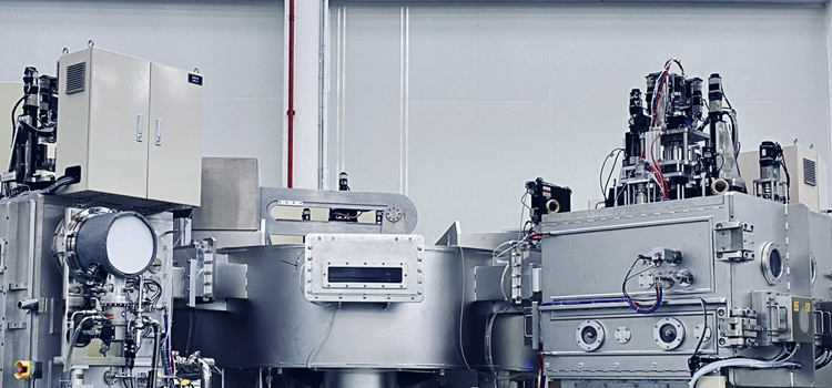
Application scenario: In the manufacturing process of Mini LED display panel and backlight (glass /PCB), inspect the bad appearance of products after die bond and furnace
Product features

– Automatic modeling according to CAD files, automatic optimization of detection path
– The minimum resolution is micron level
– Automatic normalization, accuracy up to millimeter level
– LED offset detection accuracy micron level, Angle detection accuracy <0.1°
– Real-time data interaction with die-bonder, and correct possible Die Bonding defects
– Compatible with LED position white oil and pad detection
Core Technology

– Effectively improve TT and reduce equipment vibration by COF (capture on fly) technology
– Free inspection path planning technology
– High precision inspection and measurement algorithm


 Back to list
