


 Back to list
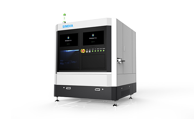
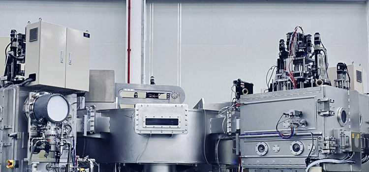
Product features

– Using high-power semiconductor laser (DPSS Laser)
– Can correspond to 2-6 inch Micro&VTF LED wafer peeling
– Unique optical path and process design ensure low GaN damage
– Laser spot Online analysis, monitoring laser status
– High precision & speed machining system up
– High precision motion and alignment system
Core Technology
– Independent intellectual property trajectory scanning
– Good control of center defects
– Online spot analysis
– Low GaN damage


Add me on Wechat
- About Us
- Company Profile
- Development History
- Company Honor
- Technology Advantage
- Sustainable development
- Main Products
- Pan-semiconductor Transfer Equipment
- Pan-semiconductor Process Equipment
- Pan-semiconductor Inspection Equipment
- Industrial Software And Big Data
- Core Components
- Contact us
-
Telephone:0551-68122312
Sales Email:sales@sineva.com.cn
HR Email:hfzp@sineva.com.cn
Address:
Between Southwest of Longzihu Rd and Jingshan Rd, Xinzhan Zone, Hefei, Anhui, 230012, China
Block 10JDB Tech Park No.18 Kechuang 10th Street BDA Beijing 100176, China
Copyright © Hefei Sineva Intelligent Machine Co.,Ltd Disclaimer Anhui ICP No.14018951 Business License
Technical Support:IBWCopyright © Hefei Sineva Intelligent Machine Co.,Ltd
Disclaimer Anhui ICP No.14018951
Business License